

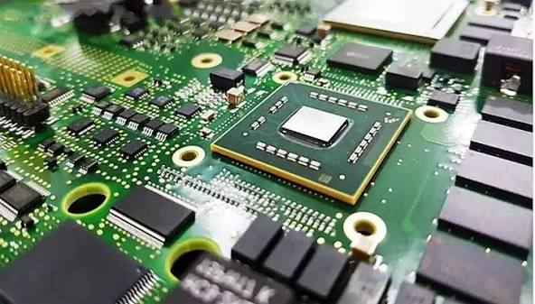
The Complexities of Advanced Component Packages
In the development of advanced electronics, from high-speed network switches to complex medical imaging systems, engineering teams increasingly rely on Ball Grid Array (BGA) and Fine-Pitch Ball Grid Array (FBGA) components. Unlike traditional perimeter-leaded packages, BGAs provide superior electrical performance, reduced inductance, and excellent thermal dissipation. However, manufacturing these high-density boards requires exceptionally tight process controls. Because the solder connections are located entirely beneath the component body, verifying the integrity of the joints becomes a significant manufacturing challenge. Relying on a highly capable Fast Turn PCB manufacturing partner ensures that these advanced packages are assembled with absolute precision, preventing costly latent failures in expensive engineering prototypes and pilot production runs.
Solder Paste Printing and Placement Accuracy
The foundation of a reliable BGA joint is established long before the board enters the reflow oven. The process begins with ultra-precise solder paste printing. Any variation in paste volume, slumping, or poor stencil release can immediately lead to catastrophic defects such as solder bridging or insufficient wetting beneath the package.
To control this critical variable, advanced fabrication facilities utilize 100% Solder Paste Inspection (SPI) immediately after the printing stage. This 3D optical scanning verifies the exact volume, height, and alignment of the paste deposits, ensuring that the foundational chemistry is absolutely perfect. Following paste application, high-speed automated placement machines must position the BGA packages with microscopic accuracy. Modern assembly lines are equipped to handle extreme miniaturization, including ultra-precise 01005 placement capabilities. Ensuring the component is perfectly aligned with the printed paste prevents the solder spheres from shifting off-pad during the transition to the reflow phase.
Optimizing the Reflow Profile for Hidden Joints
The reflow soldering stage is the most critical thermal event for a BGA package. The thermal profile must be engineered specifically for the board’s thermal mass, the specific solder alloy, and the BGA package type. If the ramp-up rate is too steep, the flux may exhaust prematurely, leading to severe oxidation and cold solder joints. If the peak temperature is held too long, the internal silicon die of the BGA can suffer permanent thermal damage.
To execute perfect metallurgical bonding, top-tier assembly partners utilize an advanced 12-zone nitrogen reflow oven. Pumping nitrogen into the reflow chamber drastically reduces oxygen levels, which minimizes oxidation during the liquidus phase. This creates superior wetting dynamics, allowing the solder spheres to collapse uniformly and form structurally sound, highly conductive electromechanical joints across the entire grid array.
Hidden-Joint Process Control and X-Ray Inspection
Even with a perfectly optimized reflow profile, the physical reality of a BGA is that its solder joints are completely invisible to the naked eye. While 100% 3D AOI (Automated Optical Inspection) is highly effective for verifying the placement, polarity, and solder fillets of standard surface-mount components, it cannot peer beneath a silicon package.
To guarantee the structural integrity of these hidden connections, rigorous BGA PCB assembly requires advanced sub-surface inspection techniques. Facilities must employ 100% X-Ray inspection for BGA, QFN, and FPGA components. High-resolution X-Ray imaging allows quality control engineers to penetrate the component body and examine the physical shape of the collapsed spheres. This critical inspection phase actively identifies hidden manufacturing defects such as excessive voiding within the joint, microscopic bridging between adjacent pads, or misalignment caused by uneven thermal expansion during reflow.
Advanced Rework Capabilities for Prototype Recovery
In the rapid prototyping phase, engineering designs are pushed to their physical limits, and occasionally, a highly complex, expensive component may need to be replaced due to a design revision or a localized failure. Without specialized equipment, attempting to remove a multi-hundred-pin BGA will inevitably destroy the underlying FR-4 substrate and severely damage surrounding microscopic components.
Instead of scrapping an entire high-value engineering build due to a single component change, specialized manufacturing facilities offer advanced BGA rework services. Using highly calibrated hot-gas rework stations, technicians can apply localized thermal profiles to cleanly desolder and lift the defective BGA without reflowing adjacent parts. The site is then meticulously prepped, and a new component is aligned using split-vision prism optics before being reflowed. This capability is a massive advantage for hardware developers, allowing them to salvage expensive prototypes, swap out upgraded FPGA silicon, and maintain their tight development schedule without ordering entirely new bare boards.
Conclusion
Successfully integrating complex BGA components into modern electronics requires an assembly partner that deeply understands the physics of solder dynamics, thermal management, and advanced defect detection. By implementing strict process controls at every single stage—from 100% SPI for paste verification to 12-zone nitrogen reflow and mandatory X-Ray inspection—manufacturers can actively eliminate the risks associated with hidden solder joints. When paired with advanced placement and precision rework capabilities, these strict manufacturing standards ensure that the most sophisticated electronic prototypes perform flawlessly in the testing lab and transition smoothly into full-scale volume production.
